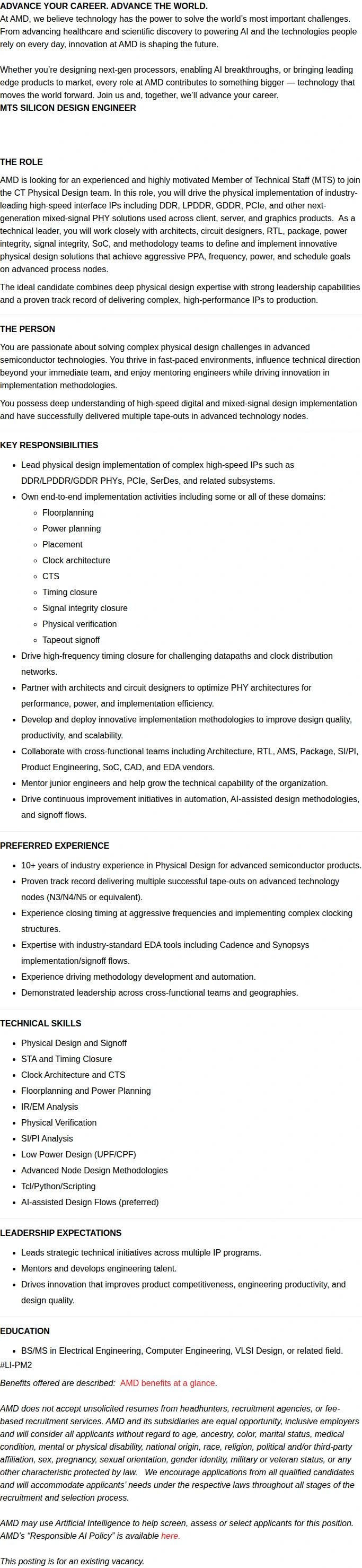
Physical Design Lead(High Speed IP's)
공고 요약
담당업무
DDR, LPDDR, GDDR, PCIe, SerDes 등 고속 인터페이스 IP physical design 구현 리드
Floorplanning, Power planning, Placement, Clock architecture, CTS, Timing closure, Signal integrity closure, Physical verification, Tapeout signoff 수행
고주파 datapath와 clock distribution network의 timing closure
PHY 아키텍처의 성능·전력·구현 효율 최적화
구현 방법론, 자동화, AI-assisted design 및 signoff flow 개발
Architecture, RTL, AMS, Package, SI/PI, Product Engineering, SoC, CAD, EDA vendor와 협업
주니어 엔지니어 멘토링 및 조직의 기술 역량 강화
자격요건
Advanced semiconductor technology 기반 physical design 및 mixed-signal design implementation 경험
N3, N4, N5 또는 동등한 advanced technology node에서 다수 tape-out 성공 경험
Aggressive frequency timing closure 및 복잡한 clocking structure 구현 경험
Cadence 및 Synopsys implementation/signoff flow 활용 역량
Physical Design, Signoff STA, Timing Closure, Clock Architecture, CTS 경험
Floorplanning, Power Planning, IR/EM Analysis, Physical Verification, SI/PI Analysis 경험
UPF/CPF 기반 Low Power Design 및 Advanced Node Design Methodologies 경험
Tcl, Python, scripting 및 methodology development·automation 경험
리더십 기대사항
여러 IP 프로그램에 걸친 전략적 기술 이니셔티브 주도
엔지니어 인재 멘토링 및 육성
제품 경쟁력, 엔지니어링 생산성, 설계 품질을 높이는 혁신 추진
교차 기능 조직과 여러 지역에 걸친 기술 리더십 발휘
마감기한
상시채용
AMD 지원하기 전 이력서 Check
시간이 없다면 AI와 한번에 수정해보세요
공고 원문